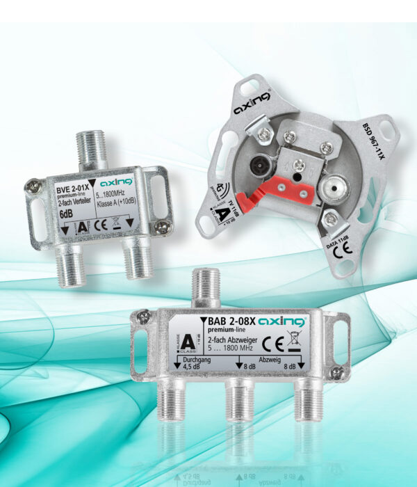
1.8 GHz passives for DOCSIS 3.1/4.0 applications
The current high-end passive components are the result of a long development phase. Many innovations have found their way, both at component level and in terms of circuit technology. In particular, the winding goods (transformers, splitters and taps) designed in-house are highly innovative and not commercially available on the market. The core materials, core geometries and winding schemes used push the limits of what is physically possible and ensure an extremely good compromise between all the values and properties listed below.
An example: A low transmission loss and good RF matching (return loss) is achieved with small cores of the winding goods. Small geometries result in short wire lengths, and the magnetic fluxes are also ideal for the RF properties. However, small cores are extremely non-linear when subjected to voltage pulses (electrostatic discharges), which leads to intermodulation and thus to a reduction in signal quality. Large cores are much better suited for the intermodulation behaviour, they can absorb voltage pulses much better, but are bad for the RF. So, if you want to use small cores, possible voltage pulses have to be absorbed externally. This requires large inductances (coils), which destroy the ideal properties of the winding material used.
Thus, the actual innovation does not lie in selectively outstanding measured values, but quite clearly in the extremely challenging combination of many very good values and properties.

Very low insertion and transmission losses:
With pass-through antenna sockets, as much of the input signal level as possible should be present at the trunk output so that subsequent antenna sockets are supplied with the best possible level.
Even with taps, as much input signal energy as possible should reach the trunk output.
In the case of splitters, the input signal level should be distributed as evenly as possible to the outputs and with minimal loss of energy or level.

Example 1: Pass-through attenuation IN to OUT of a multimedia pass-through socket BSD 967-20X; 1dB and less at low frequencies and only 2dB at the upper frequency band limit of 1.8GHz
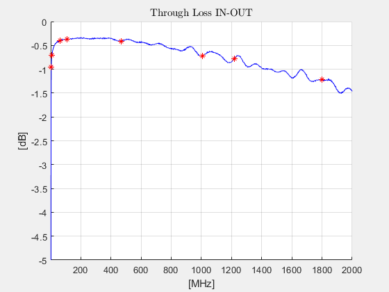
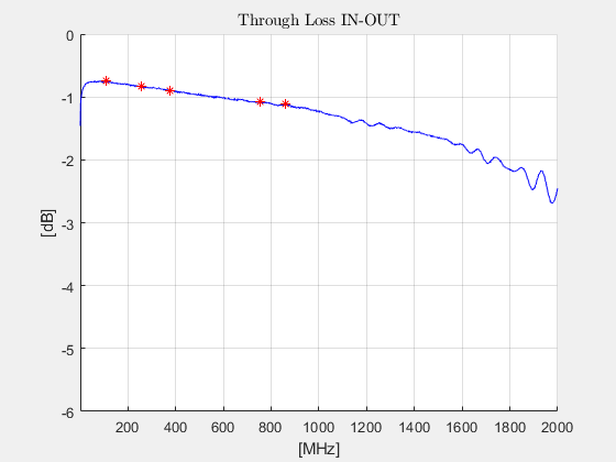
Example 2: Through loss IN to OUT of a single tap BAB 1-20X; well under 1 dB at low frequencies and just 1.2 dB at the upper frequency band limit of 1.8 GHz
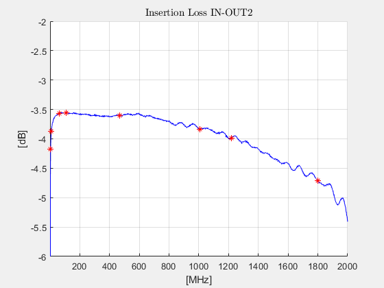
Example 3: Distribution attenuation IN to OUT2 of a two-way splitter BVE 2-01X
The theoretical minimum distribution loss is calculated as 10*log(2) = 3.01 dB
At low frequencies, the AXING component is only around 0.5 dB above what is theoretically achievable value
Even at the upper frequency band limit of 1.8 GHz, the current component only attenuates 4.7 dB
Very linear frequency response:
Ideally, a frequency response is absolutely flat and “smooth”, which means that all frequencies are equally “strong”, i. e. transmitted with the same signal level. In reality, this is not possible due to various non-idealities of components and materials. Physics and the laws of nature also play an important role. For example, when transmitting signals over any transmission medium (e. g. coaxial cable, air, conductor track on a circuit board, vacuum, etc.), high frequencies are generally more strongly attenuated than low ones. You can’t circumvent the laws of nature! You can only work on keeping component non-idealities as low as possible through the construction and the materials used and to come as close as possible to the physical limits.
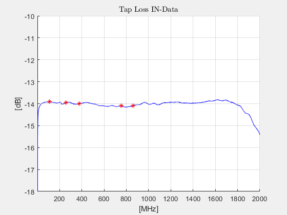
Example 1: Tap attenuation IN to DATA of a multimedia pass-through socket BSD 967-14X
The tap is realized via a directional coupler. Since the 14 dB tap attenuation is desired with a “14-dB-through-socket” and value is not placed on maximum level yield, it is possible to design the frequency response to be extremely linear. This requires extremely good directional couplers that guarantee extremely high linearity up to 1.8 GHz.
Example 2: Pass-through attenuation IN to OUT of a multimedia pass-through socket BSD 967-20X
A maximum level output is desired in the pass-through path of a socket. Physical effects at high frequencies have a major impact here. In addition to the very low absolute insertion loss already mentioned, this example also shows that high frequencies are transmitted only slightly “worse” than low frequencies!
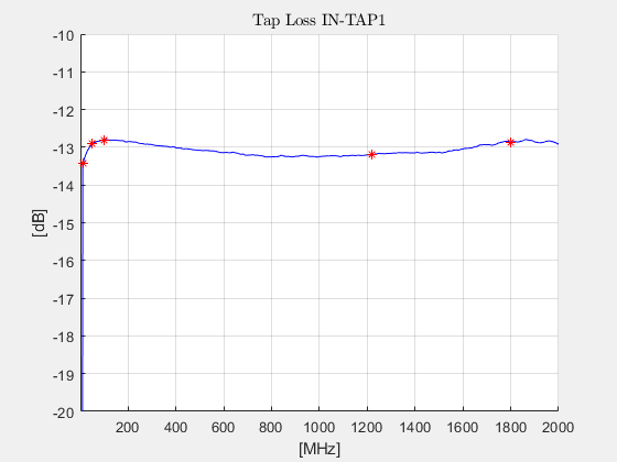
Example 3: Frequency response at the 13 dB tap output number 1 of an 8-way graded tap BAB 8-01X
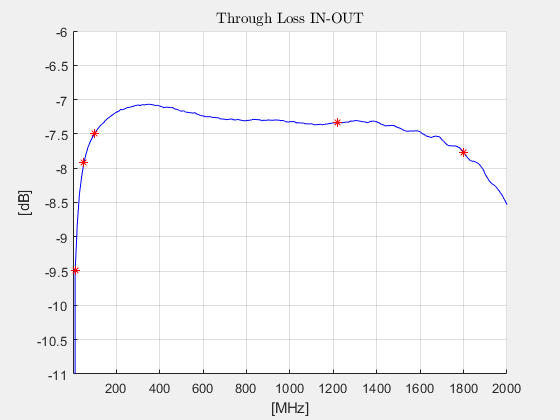
Example 4: Frequency response from input to output of an 8-way graded tap BAB 8-01X
A so-called “graded tap” is a component with several outputs (8 in the example shown), which has a 1 dB higher tap loss at each tap output (13 to 20 dB in the example shown). This is implemented in the component by a chain of individual directional couplers. Thus, with an 8-way graded tap, the input signal passes through 8 directional couplers to the output! Nevertheless, the signal at the output in the example on the left shows extremely low ripple of less than 1 dB over the entire frequency range up to 1.8 GHz. In addition to the low ripple, the extremely low absolute transmission loss of around 7.3 dB on average should be emphasized once again. This is an extremely low value after going through 8 (!) directional couplers.
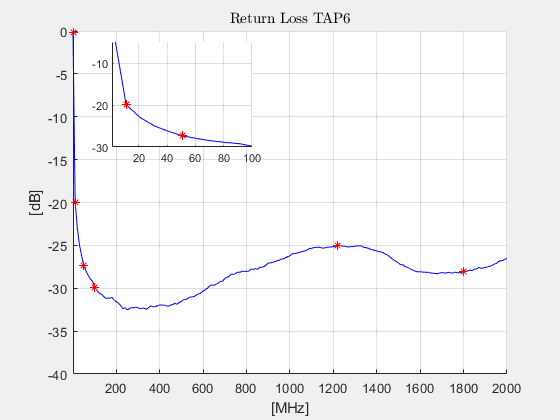
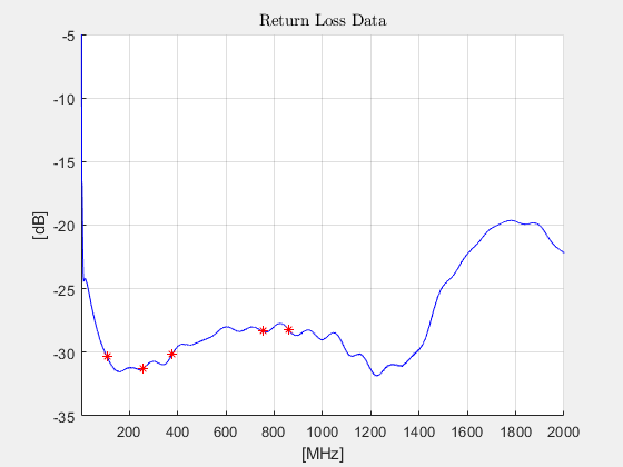
Very good return loss:
Ideally, RF components in communications technology have what is known as a characteristic wave impedance of 75 ohms. This ensures that the signals in a chain of components and cables are transmitted as perfectly and loss-free as possible.
In reality, this characteristic wave impedance sometimes deviates from 75 ohms and is also frequency dependent. If the characteristic impedance deviates from 75 ohms at one point in a transmission system, reflections occur. The RF signal energy traveling from the source to the sink cannot fully overcome the jump in characteristic impedance and signal components travel back down the line in the direction from which they originally came. Ultimately, this leads to level losses and ripples in the frequency response, especially if the characteristic impedance is violated at several points in the transmission system.
Return loss is a measure of how well the characteristic wave impedance of an RF device at a given frequency matches the ideal 75 ohms. The return loss describes in a negative dB quantity how much signal energy is reflected at a port (input or output) of a component. The larger the value for the adjustment in -dB, the more ideally a component behaves. This means: a value of, for example -6 dB corresponds to a poor impedance matching and a value of, for example -14 dB corresponds to a good (but not outstanding) matching / return loss.
Example 1: Return loss at the input of a 2-way tap BAB 2-08X with 8 dB tap attenuation at the two outputs
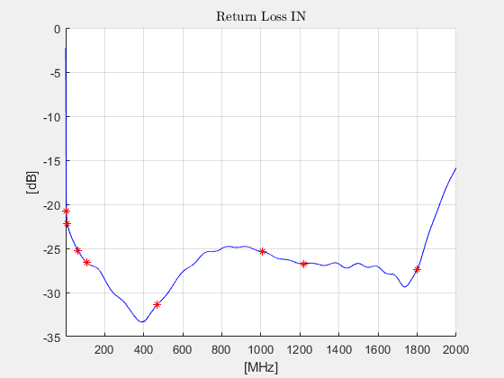
Example 2: Return loss at tap output number 6 of an 8-way graded tap BAB 8-01X
Example 3: Return loss at the DATA port of a multimedia pass-through socket BSD 967-20X
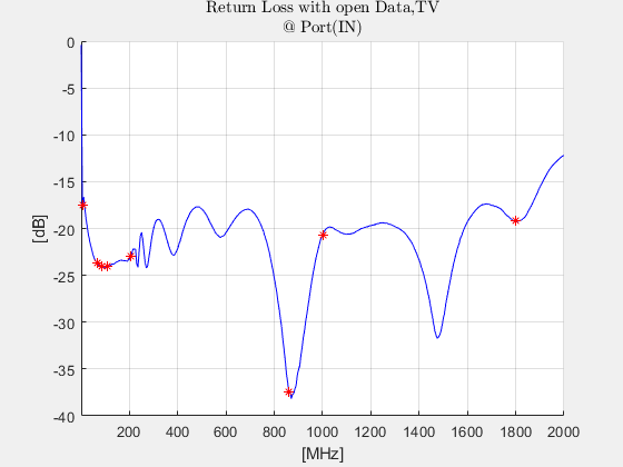
Example 4: Return loss at the input of a BSD 967-20X multimedia pass-through socket with non-terminated outputs and ports.
Normally, the return loss / matching is measured in one port of a component when all other ports are ideally terminated with 75 ohms. In the case of antenna sockets, however, this may not be the case in practice, for example because no devices are connected (modem, TV set) or because no coaxial cable is routed from a through socket to other sockets. Especially free output ports are common practice with antenna sockets, since two devices (modem and TV) are not connected to every socket in an apartment. In the rarest of cases, unused ports are provided with terminating resistors.
The latest AXING antenna sockets are characterized by the fact that a very good return loss is achieved even when not used as intended! This has extreme advantages because the distribution network is not deteriorated.
High port-to-port isolation:
The ports of passive components should be isolated as well as possible from an RF perspective. This is essentially necessary for two reasons.
- If a cable modem is operated at a port of a component in network level 4, it transmits with considerable levels of up to 118 dBµV based on a 6.4 MHz bandwidth. These high levels should not disturb the devices (TVs, STBs, modems) operated on other ports of the same component.
- It may happen that e. g. through poorly shielded end devices (TVs, modems, inferior STBs), through poorly shielded receiver connection cables or through improper use (e. g. a wire that is inserted into a port of an antenna socket and acts like an antenna) interference couples into the transmission system. A popular source of interference with a high RF radio level is, for example, mobile radio devices, but other sources such as lamps and lights, machines or household appliances can also generate RF interference energy. The interference that is coupled in should not disturb the devices (TVs, STBs, modems) operated on other ports of a passive component.
The isolation, i. e. the attenuation between two ports, which should ideally be independent of each other, is specified in dB. The greater the magnitude of this value, the better the decoupling between the two ports measured.
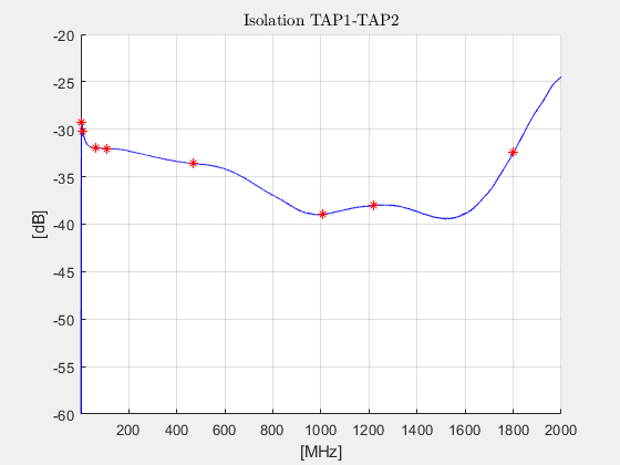
Example 1: Isolation of the two outputs of a 2-way tap BAB 2-08X with 8 dB tap attenuation at the two outputs; the isolation is > 30 dB at every frequency! In the case of taps (including components with more than two tap outputs), the isolation between adjacent ports is the most critical due to the design. The further apart the branches are, the better the isolation will be (see next example).
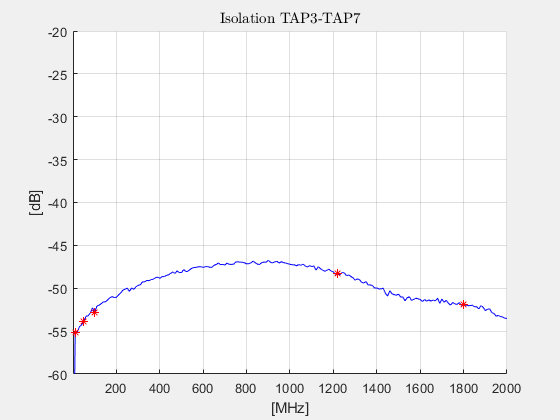
Example 2: Isolation between outputs 3 and 7 of an 8-way graded tap BAB 8-01 X; values of better than 45 dB are achieved
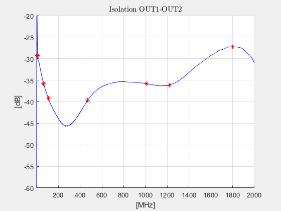
Example 3: Isolation of the two outputs of a 2-way splitter BVE 2-01X.
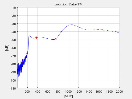
Example 4: Isolation between the TV and DATA port of a multimedia pass-through socket BSD 967-11X
Very high surge protection:
All passive components are immune to the following voltage pulses:
- 1 kV / 1.2/50 µs surge pulse according to IEC 61000-4-5
- 160 VDC pulse (for magnetization before intermodulation measurement (see next point))
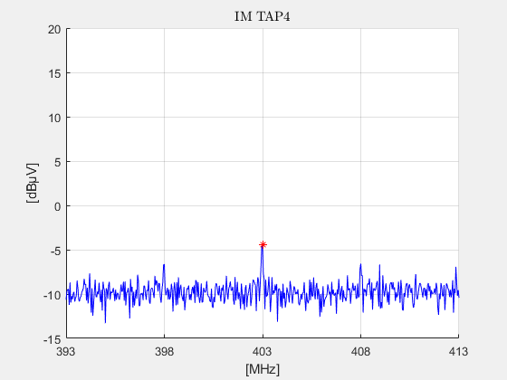
High intermodulation immunity (≤ 115 dBc):
Intermodulation means that non-linear effects can result in mixing products. This means that signals can arise on new frequencies that were not initially present in the original signal. The simplest possible test signals, i. e. sine carriers (CW), are used to test the tendency of a component for signals to intermodulate on it and to obtain a defined measured value. A passive component is subjected to two high-level sine-wave carriers at two frequencies. Then at the frequencies where one would expect mixing products – this is, among others, at the sum or difference of the two test frequencies (f1 ± f2) as well as at the double of a test frequency plus or minus the other frequency (2*f1 ± f2, 2*f2 ± f1) the case – measured and the value determined by how much weaker the intermodulation products are than the two test signals. The result is a value with the unit dBc. This stands for “dB below carrier” and thus indicates how many dB lower the mixing products are than the level of the test carrier. A value of 115 dBc means that the mixing products are 115 dB lower than the level of the test frequencies.
These values are kept even after the components have been subjected to the aforementioned voltage / surge pulses. The winding goods, whose cores are responsible for increased intermodulation after voltage pulses, are highly immune to external voltage pulses, both due to their construction and their surrounding circuitry. The art here is that the high intermodulation resistance does not have a too negative effect on the RF parameters of the components!
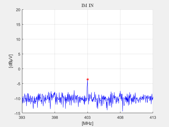
Example 1: Intermodulation at the input of a multimedia end socket BSD 967-04X; 123.7 dBc (since test carrier level = 120 dBµV)
Example 2: Intermodulation at tap output number 7 of an 8-way graded tap BAB 8-01X; 124.5 dBc (since test carrier level = 120 dBµV)